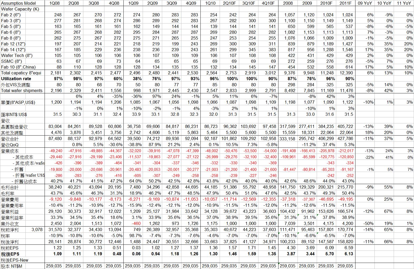
營收: 1,000E~1,020E, +8.5~10.6%
GP%: 48~50%
OP%: 36.5~38.5%
依此推算:
UTR: 100%
Wafer shipments: 2,833K, +11% QoQ
ASP: US$1,087, +2% QoQ
但因為NT$/US$假設為31.3(1Q10 31.96),所以營收只+10.5% QoQ
Moore’s Law
Moore’s Law至少還有10年,而10年之後如果Moore’s Law停止了,製程演進走到盡頭,TSMC還有另外10年的研發優勢,可以在將特定製程針對各種應用增加功能(features),例如現在的先進製程是45/40nm(Intel的32nm),但是各種特定的功能應用例如Embedded memory, CMOS image sensor, Analog, Mixed-mode, RF, MEMS, Power management, Display driver等等,製程都遠遠落後45/40nm,還是需要研發增加功能才能切入這些特定應用的市場。也就是說,TSMC的研發優勢至少還可以延續20年。
又例如,Morre’s Law變慢或停止了,但是system integration的趨勢還是會繼續進行,因此SoC就會從現在的System on die, 變成System in package(SIP),TSMC必須要提供一個平台讓客戶可以繼續整合,因此切入(1)wafer level package, 從2D to 3D(立體封裝), (2)Silicon substrate等技術。
28nm技術時程
(1)28LP, low power, SiNO, Gate-First, 2010/6
(2)28HP, high performance, HKMG, Gate-Last, 2010/9
(3)28HPL, low power, HKMG, Gate-Last, End-2010
(4)28HPM, 希望兼顧high performance和low power,目標市場在於行動運算CPU,例如Smartphone or MID
Gate-Frist和Gate-Last之爭
針對Gate-First和Gate-Last之爭,目前選擇Gate-Last的只有TSMC和Intel,IBM陣營包括Samsumg, Global foundry, Chartered和一些IDM廠則選擇Gate-First,IBM陣營宣稱Gate-First做出來的die size比較小,製程上也有成本優勢,而且研發比較容易成功,但也承認比較適合low power, performance應用比較差,而蔣尚義認為,Gate-Last的製程步驟(process steps, 將影響cycle time, 而cycle time將影響成本)、和光罩層數(mask level)都和Gate-First類似,因此成本不會比較高,至於影響die size的design rule,和gate-first/gate-last無關,因此Gate-Last的die size也不會比較大,但是比較難做是真的,如果你學會的話,performance比較好,也不會比較貴。
蔣尚義大膽預測,Gate-Last終必成功,到了22/20nm,IBM陣營的對手們將全部轉回來做Gate-Last,將可證明他們選擇錯誤,蔣先生似乎暗示,對手陣營中,很快就會有人率先開始重新研發28nm的Gate-Last。
如果蔣先生所言不虛,則表示Globalfoundries和Chartered用Gate-First做需要hign performance的CPU,會比TSMC的Gate-Last差,那麼,AMD(PC)、IBM的CPU(Game),可能就會有大問題了,AMD採用Bulk CMOS的CPU是否也被迫要轉單到TSMC? 未來一大堆ARM-based或MIPS-based的RISC CPU,是不是也都必須到TSMC投片?
RRB(Richard's Research Blog)查了一下Globalfoundries的網站,有這麼一段話:
The "Gate Last" approach to HKMG is costly and requires a number of additional processing steps. GLOBALFOUNDRIES has chosen to implement a "Gate First" approach because it is simpler and more scalable to future generations. The process flow is very similar to what was used for previous technology generations. The "Gate First" maximizes power efficiency and transistor scaling while minimizing die size and design complexity when compared to the alternative "Gate Last" approach.
http://www.globalfoundries.com/technology/tech_elements.aspx
很明顯的,Globalfoundries的說法和TSMC的說法剛好相反,事實只有一個,不是有人說謊,就是有人功力不夠,看得不透徹,以至於選錯技術路線,當然,RRB相信TSMC,畢竟,蔣先生當年在0.13um天險的銅製程Black Diamond和SILK之爭,曾經大敗IBM和U聯軍,讓TSMC在0.13um世代之後取得絕對的技術領先優勢,兩年多前張先生把已半退休的蔣先生找回來重新掌管RD,會不會再度大敗IBM聯軍,我們拭目以待。
這個議題對未來兩年foundry的競爭,甚至半導體業的競爭,應該都非常重要,很奇怪好像很少人關心這件事,大部份報告和媒體都沒有提。
2 則留言:
what I think is same with you.
Due to Intel is alwaye the process tech leader (not tsmc), so if Intel think gate last is better; I do believe they are right. Just gate last cost should be little higher than gate first (more process).
leonchang123@yahoo.com.tw
Thnaks for your comments
張貼留言
注意:只有此網誌的成員可以留言。